New Materials and Analysis

Material in micro view

Groundbreaking analytical methods and modifications for tomorrow’s materials

New materials are at the heart of innovation – whether in energy, mobility, electronics, or medical technology.
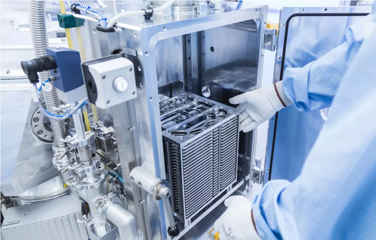
To understand them in depth and develop them with precision, advanced analysis and modification techniques are essential. Hi-Acts enables exactly that: industry–science partnerships for deep insights into tomorrow’s materials – with access to leading accelerator-based technologies, cutting-edge infrastructure, and scientific expertise.

Overview

Spanner includes round material
New Materials

1. Optimise Materials and Surfaces

- Ion implantation for Enhanced Performance: Use of high-energy ion beams to modify the physical and electrical properties of semiconductor materials.

- Surface Processing by Ion Bombardment: Material removal by bombardment of a solid body with energetic ions (ion erosion or ion sputtering).

2. Nanostructures for Innovative Applications

- Customised Membranes for Sensor Technology and Filtration: The production of membranes with precisely defined nano- and micropores, created by irradiation with high-energy heavy ions followed by chemical etching.

- Customised nanowires for electrochemistry and catalysis:  Controlled production of nanowire arrays and complex nanonetworks.

Examples of Applications and Cases
Success Story Ion Implantation
High-energy ion implantation as a foundry service for the global power semiconductor industry

The Ion Beam Centre (IBC) at the Helmholtz-Zentrum Dresden-Rossendorf HZDR offers many years of expertise in ion implantation, modification and analysis. The HZDR Innovation GmbH is making it much more accessible, e. g. for microelectronics. Read more!

Learn more
Abstract particles in light
Ion Implantation and Modification of Materials

The working group operates specialised equipment that can be used to modify and improve material surfaces in a targeted manner using ion beams – even on components with diameters of up to 200 millimetres. The process is used for both industrial projects and research and makes it possible to precisely adjust properties such as hardness, wear and corrosion resistance, and electrical conductivity – for example, in semiconductor manufacturing.

Learn more
Abstract Artist's Impression of Nanoparticles forming structures.
Ion Induced Nanostructures

The research focuses on processes in which low-energy ions specifically alter material surfaces – for example, for cleaning, smoothing, roughening or producing extremely fine nanostructures. Depending on the process used, materials can be precisely ablated, modified or restructured, enabling a wide range of applications in technology and research.

Learn more
Abstract structure made out of thin holes.
Ion Track Membranes

When materials are irradiated, high-energy ions create ion tracks, which can be chemically etched into open channels in polymers. These ion track membranes can be specifically functionalised and used as templates for the production of nanowire structures.

Learn more
Contact us for any further information

JOHANNES BLUM

Innovation Manager

Would you like to discuss our range of services? Then give us a call or arrange an appointment with one of our innovation managers.

Submit your request nowJohannes Blum